
Power semiconductor course (SiC/GaN)
About our
Power Semiconductors (Sic/Gan) Course
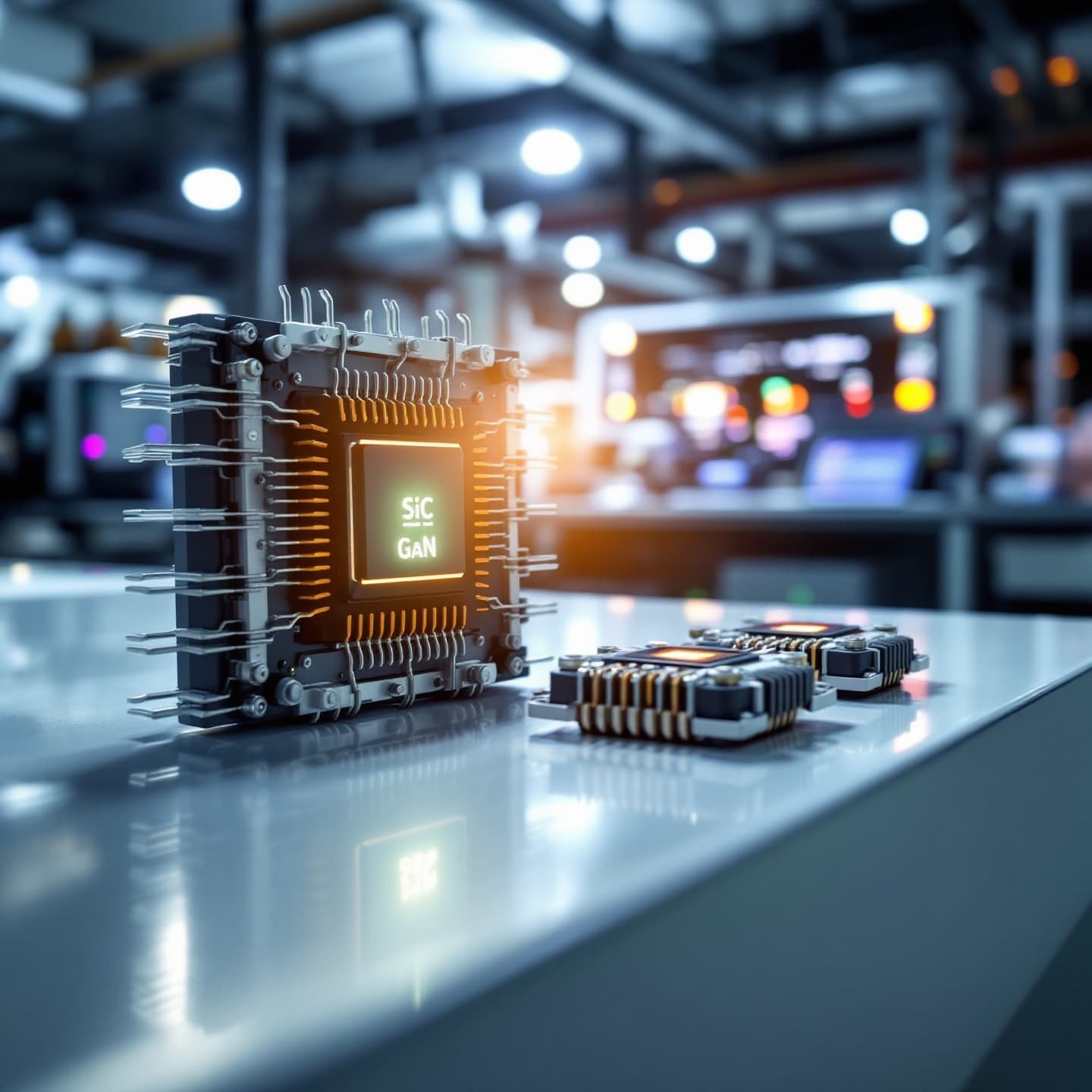
Explore the cutting edge of power electronics, focusing on silicon carbide (SiC) and gallium nitride (GaN) materials. The course delves into the design, fabrication, and application of devices based on these technologies, including MOSFET transistors and Schottky diodes, optimized for high efficiency and high frequencies. The course covers the analysis of the electrical characteristics, thermal performance, and reliability of these advanced semiconductors, as well as their integration into power converters, inverters, and energy management systems, considering industry standards and emerging applications.
The program offers a practical approach through simulations, laboratories, and case studies in areas such as electric vehicles (EVs), renewable energy, and smart grids. Knowledge of power control and circuit protection techniques, essential for the application of SiC/GaN devices, is provided. Participants acquire the skills necessary for the selection, design, and implementation of solutions based on these semiconductors, enhancing their professional profile in constantly evolving industries.
Power semiconductor course (SiC/GaN)
- Format: Hybrid
- Duration: 3 months
- Hours: 300 H
- Language: English / Spanish
- Registration date: 23-10-2026
- Start date: 12-12-2026
- Available places: 3
399 $
Competencies and results
What you will learn
1. Advanced Analysis of SiC/GaN Power Devices: Design, Simulation and Applications
- Fundamentals of SiC and GaN Broadband Semiconductors: Structure, Properties, and Advantages in Power Applications.
- Modeling and Simulation of SiC/GaN Devices: Device Models, Simulation Tools (SPICE, etc.), and Performance Analysis.
- Circuit Design with SiC/GaN Devices: Power Converters (DC-DC, DC-AC, AC-DC), Inverters, and Control Systems.
- Switching and Loss Analysis in SiC/GaN Devices: Transient Modeling, Efficiency, and Thermal Management.
- Practical Applications of SiC/GaN Devices: Power Supplies, Motor Drives, Electric Vehicles, Renewable Energy, and More.
- Design and Optimization of Heat Sinks for SiC/GaN Devices: Thermal Analysis, Material Selection, and Cooling Strategies.
- Reliability and Durability Analysis of SiC/GaN Devices: Aging Tests, Analysis of Failures and mitigation strategies.
Integrating SiC/GaN devices into systems: PCB design, electromagnetic shielding, and compatibility.
Regulations and standards related to SiC/GaN devices: regulatory compliance and safety.
Future trends and advances in SiC/GaN technology: ongoing research and development.
2. Comprehensive Domain of SiC/GaN Semiconductors: Fundamentals, Implementation and Optimization
Here is the requested content:
- Understand SiC and GaN semiconductor technology: its properties, advantages, and applications.
- Analyze the fundamentals of semiconductor physics and its application to SiC/GaN.
- Study the structures of SiC/GaN devices: diodes, transistors, and other components.
- Learn about SiC/GaN manufacturing processes and growth techniques.
- Explore the electrical characteristics of SiC/GaN devices: switching, efficiency, and performance.
- Design and implement circuits using SiC/GaN devices for various applications.
- Optimize circuit design to minimize losses and maximize efficiency.
- Analyze the thermal and temperature management aspects of SiC/GaN systems.
- Understand device protection and reliability techniques SiC/GaN.
Study the practical applications of SiC/GaN in power electronics, communications, and other industries.
Evaluate the performance and efficiency of SiC/GaN circuit designs.
Use simulation tools for the design and analysis of SiC/GaN circuits.
Learn about the trends and future of SiC/GaN technology.
3. Comprehensive user-oriented design and validation (from modeling to manufacturing)
You will learn to integrate the entire product development process, from initial model conception to final validation, applying user-centered methodologies. You will develop skills in parametric design, ergonomics, simulation, sustainable materials, 3D visualization, and manufacturing management, ensuring efficient, safe solutions that meet current industry standards.
4. In-depth Exploration of SiC/GaN Technology: Principles, Modeling and Strategic Applications
4. In-Depth Exploration of SiC/GaN Technology: Principles, Modeling, and Strategic Applications
Master the fundamentals of silicon carbide (SiC) and gallium nitride (GaN) semiconductors: crystal structure, physical and chemical properties, and key differences from silicon (Si).
Understand the manufacturing processes of SiC and GaN devices: crystal growth, epitaxy, lithography, etching, and metallization.
Analyze the operating principles of SiC and GaN devices: Schottky diodes, MOSFETs, HEMTs, and their performance characteristics (breakdown voltage, current, switching frequency, efficiency).
Study the modeling of SiC and GaN devices: physical and compact models, circuit simulation, and software tools (e.g., SPICE, TCAD).
Explore the strategic applications of SiC/GaN technology in various Sectors:
- Power electronics: power converters, inverters, electric vehicle (EV) chargers, high-efficiency power supplies.
- Wireless communications: RF power amplifiers for 5G/6G base stations, radars, satellites.
- High-temperature electronics: aerospace, automotive, and industrial applications.
Study practical cases and examples of real-world applications of SiC/GaN technology in different industries.
5. SiC/GaN Power Semiconductor Engineering: Design, Simulation, Characterization and Applications
5. SiC/GaN Power Semiconductor Engineering: Design, Simulation, Characterization, and Applications
- Fundamentals of SiC and GaN power semiconductors: structure, properties, and advantages.
- Modeling and simulation of SiC/GaN devices: advanced tools and techniques.
- Design of circuits with SiC/GaN semiconductors: DC-DC, DC-AC, and AC-DC converters.
- Characterization of SiC/GaN devices and circuits: electrical and thermal measurements.
- Applications of SiC/GaN semiconductors in power electronics: energy efficiency and miniaturization.
- Design of thermal management systems for SiC/GaN devices: cooling and heat dissipation.
- Failure analysis and reliability of SiC/GaN semiconductors: degradation mechanisms and mitigation strategies.
- Integration of SiC/GaN semiconductors in specific applications: electric vehicles, renewable energy, and industry.
- Regulations and standards in the design and manufacture of SiC/GaN devices and systems.
- Future trends and challenges in SiC/GaN power semiconductor engineering.
6. Optimization of Electrical Systems with SiC/GaN Semiconductors: Analysis, Simulation and Strategic Development
6. **Optimization of Electrical Systems with SiC/GaN Semiconductors: Analysis, Simulation, and Strategic Development**
Understand the underlying physics and key characteristics of silicon carbide (SiC) and gallium nitride (GaN) semiconductors, including their crystal structure, carrier transport properties, and thermal behavior.
Analyze the comparative advantages and disadvantages of SiC and GaN in power electronics applications, considering factors such as efficiency, power density, switching speed, and cost.
Master numerical simulation techniques for the design and analysis of SiC- and GaN-based power circuits, using industry-standard simulation tools such as SPICE and finite element analysis (FEA) simulators.
Model and simulate key power electronics components, such as diodes, MOSFET transistors, and integrated power modules (IPMs), based on SiC and GaN, with an emphasis on the analysis of transients and performance optimization.
Design and optimize power converters (AC-DC, DC-DC, DC-AC) using SiC and GaN semiconductors, considering aspects such as circuit topology, PWM modulation, component selection, and thermal management design.
Evaluate and mitigate noise and EMI (Electromagnetic Interference) problems in SiC and GaN-based power systems by implementing filtering, shielding, and PCB design techniques.
Implement advanced control strategies for power converters, including predictive control, sliding mode control, and digital control, to improve performance and efficiency.
Analyze and optimize the thermal performance of SiC and GaN-based power systems using heat sinks, liquid cooling techniques, and heat transfer simulation.
Explore specific applications of SiC and GaN in different industries, such as the automotive industry. (electric and hybrid vehicles), renewable energy (solar panels, wind turbines), consumer electronics, and the aerospace industry.
Develop a design strategy for the development of SiC and GaN-based electrical systems, from component selection and circuit design to manufacturing, testing, and certification.
Understand current and future trends in SiC and GaN semiconductor technology, including the development of new materials, device structures, and emerging applications.
Who this program is for:
Power semiconductor course (SiC/GaN)
- Engineers with degrees in fields such as Electrical Engineering, Electronics, Telecommunications, or similar disciplines.
- Professionals working in the design, development, or maintenance of power systems, including but not limited to: design engineers, application engineers, and specialized technicians.
- Experts in key industries such as: automotive (electric and hybrid vehicles), renewable energy (solar panels, wind turbine inverters), and power electronics in general.
- Researchers, academics, and graduate students with an interest in SiC/GaN technologies and their application in power devices.
Recommended requirements: Basic knowledge of electronics, circuits, and semiconductors. Familiarity with semiconductor physics concepts and/or experience in circuit simulation.
English proficiency at level B2 or higher for understanding technical materials and participating in the course.
- Standards-driven curriculum: you will work with CS-27/CS-29, DO-160, DO-178C/DO-254, ARP4754A/ARP4761, ADS-33E-PRF from the first module.
- Accreditable laboratories (EN ISO/IEC 17025) with rotor bench, EMC/Lightning pre-compliance, HIL/SIL, vibrations/acoustics.
- Evidence-oriented TFM: safety case, test plan, compliance dossierand operational limits.
- Mentored by industry: teachers with experience in rotorcraft, tiltrotor, eVTOL/UAM and flight test.
- Flexible modality (hybrid/online), international cohorts and support from SEIUM Career Services.
- Ethics and security: safety-by-design approach, cyber-OT, DIH and compliance as pillars.
Module 1 — Advanced Analysis of SiC/GaN Power Devices: Design, Simulation, and Applications
1.1 Fundamentals of SiC and GaN Semiconductors: Structure, Properties, and Advantages
1.2 Design of SiC/GaN Power Devices: MOSFETs, JFETs, and Diodes
1.3 Modeling and Simulation of SiC/GaN Devices: Advanced Tools and Techniques
1.4 Characterization of SiC/GaN Devices: Measurements and Analysis of Key Parameters
1.5 Applications of SiC/GaN Devices in Power Converters: Topologies and Designs
1.6 Design of Drive Circuits for SiC/GaN Devices: Optimization and Protection
1.7 Loss and Efficiency Analysis of SiC/GaN Devices: Modeling and Simulation
1.8 Cooling Techniques for SiC/GaN Devices: Heatsink Design and Selection 1.9 Advanced applications of SiC/GaN: inverters, DC-DC converters, and chargers.
1.10 Case studies and practical examples of design and simulation with SiC/GaN.
2.2 Fundamentals of SiC/GaN Semiconductors: Structure and Properties
2.2 SiC vs. GaN Comparison: Advantages and Disadvantages in Power Applications
2.3 Manufacturing Process: From Base Material to Final Device
2.4 Characterization of SiC/GaN Devices: Key Parameters and Measurements
2.5 Device Modeling: Circuit Simulation and Analysis
2.6 Implementation of SiC/GaN Devices in Power Systems
2.7 Circuit Optimization: Driver and Protection Design
2.8 Thermal Considerations: Heat Dissipation and Management
2.9 Optimization Techniques: Switching, Efficiency, and Performance
2.20 Practical Applications and Case Studies
3.3 Fundamentals of SiC/GaN Circuit Design: Basic Topologies and Component Selection
3.2 Modeling and Simulation of SiC/GaN Circuits: Simulation Tools and Techniques
3.3 Design of SiC/GaN DC-DC Converters: Efficiency and Performance Optimization
3.4 Design of SiC/GaN Inverters: Switching and Control Strategies
3.5 Applications of SiC/GaN Circuits in Power Electronics: Power Supplies and Motor Drives
3.6 Design of Protection Circuits for SiC/GaN Devices: Overvoltages and Overcurrents
3.7 Thermal Design and Heat Dissipation Management in SiC/GaN Circuits
3.8 Design of Control Circuits and Gate Drivers for SiC/GaN
3.9 Practical Applications: Analysis of Case Studies and Real-World Examples
3.30 Implementation and Testing of SiC/GaN Circuits: Methodology and Design Verification
4.4 Fundamentals of SiC/GaN Semiconductors: Structure and Properties
4.2 Modeling SiC/GaN Devices: Simulation Models and Key Parameters
4.3 Strategic Applications of SiC/GaN in Energy Conversion: Design and Optimization
4.4 Operating Principles of SiC/GaN Power Switches
4.5 Applications in Electric Propulsion Systems
4.6 Applications in Electric and Hybrid Vehicles
4.7 Applications in High-Efficiency Power Supplies
4.8 Integration and Design of SiC/GaN Circuits
4.9 Comparison of SiC/GaN vs. Silicon in Power Applications
4.40 Future Trends and Challenges in SiC/GaN Technology
5.5 SiC/GaN Device Design Principles
5.5 SiC/GaN Device Modeling: Analysis and Simulation
5.3 Power Circuit Design with SiC/GaN
5.4 SiC/GaN Power Converter Applications
5.5 SiC/GaN Device Characterization and Testing
5.6 Control Systems for SiC/GaN Applications
5.7 Thermal Design in SiC/GaN Systems
5.8 SiC/GaN PCB Integration and Design
5.9 High-Frequency System Design with SiC/GaN
5.50 Industrial and Renewable Energy Applications with SiC/GaN
6.6 Energy Efficiency Analysis in SiC/GaN Power Systems
6.2 Simulation of Charge and Discharge Scenarios in SiC/GaN Applications
6.3 Development of Control Strategies for SiC/GaN System Optimization
6.4 Design of Filters and Protection Circuits for Optimized SiC/GaN Systems
6.5 Thermal Optimization and Heat Management in SiC/GaN Systems
6.6 SiC/GaN Applications in Power Inverters and Converters
6.7 Evaluation of the Impact of SiC/GaN on the Efficiency of Electrical Systems
6.8 Reliability and Durability Analysis of Optimized SiC/GaN Systems
6.9 Strategic Development of SiC/GaN Solutions for Different Industries
6.60 Case Studies: Real-World Applications and Future Trends in SiC/GaN Systems
- Hands-on methodology: test-before-you-trust, design reviews, failure analysis, compliance evidence.
- Software (depending on licenses/partners): MATLAB/Simulink, Python (NumPy/SciPy), OpenVSP, SU2/OpenFOAM, Nastran/Abaqus, AMESim/Modelica, acoustics tools, planning toolchains DO-178C.
- SEIUM Laboratories: scale rotor bench, vibrations/acoustics, EMC/Lightning pre-compliance, HIL/SIL for AFCS, data acquisition with strain gauging.
- Standards and compliance: EN 9100, 17025, ISO 27001, GDPR.
Capstone-type projects
- Motor Control with SiC/GaN: Optimized PWM design, efficiency, and EMI reduction.
- SiC/GaN Power Conversion: Inverter simulation, topology optimization, and industrial applications.
- SiC/GaN Power Supply Systems: Semiconductor integration, thermal management, and performance testing.
- SiC/GaN Applications: Prototype development and cost-benefit analysis.
- Advanced Design of SiC/GaN Converters: Topologies, simulation, and prototyping for energy efficiency.
- SiC/GaN Intelligent Modeling and Control: Predictive algorithms and performance optimization.
- Integration of SiC/GaN in Naval Power Systems: Analysis, simulation, and specific applications.
- SiC/GaN Thermal Analysis and Reliability: Dissipation design and life evaluation.
- SiC/GaN Converter Design: Simulation, prototyping, and efficiency for specific applications.
- SiC/GaN Intelligent Control: Adaptive control strategies to optimize performance.
- SiC/GaN Applications in Electric Vehicles: Design of high-efficiency inverters and chargers.
- Advanced Modeling and Simulation: Creation of accurate models and simulations to validate designs.
- Advanced Design of SiC/GaN Converters: Topologies, Simulation, and Efficiency.
- Intelligent Control of SiC/GaN Motors: Algorithms, Optimization, and Applications.
- SiC/GaN System Integration: PCB Design, Thermal Management, and Reliability.
- SiC/GaN Validation and Characterization: Testing, Analysis, and Energy Applications.
Admissions, fees, and scholarships
- Profile: Background in Computer Engineering, Mathematics, Statistics, or related fields; practical experience in NLP and valued information retrieval systems.
- Documentation: Updated CV, academic transcript, SOP/statement of purpose, project examples or code (optional).
- Process: Application → Technical evaluation of profile and experience → Technical interview → Review of case studies → Final decision → Enrollment.
- Fees:
- Single payment: 10% discount.
- Payment in 3 installments: No fees; 30% upon registration + 2 equal monthly payments of the remaining 35%.
Monthly payment: available with a 7% commission on the total; annual review.
Scholarships: based on academic merit, financial need, and promoting inclusion; agreements with companies in the sector for partial or full scholarships.
See “Calendar & Calls for Applications,” “Scholarships & Grants,” and “Fees & Financing” in the SEIUM mega-menu.
Do you have any questions?
Our team is ready to help you. Contact us, and we will respond as soon as possible.
F. A. Q
Frequently asked questions
Yes, we have international certification
Yes: experimental models, real data, applied simulations, professional environments, real case studies.
It is not mandatory. We offer leveling tracks and tutoring.
Completely. It covers e-propulsion, integration, and emerging regulations (SC-VTOL).
Recommended. There are also internal challenges and consortiums.
Yes. Online/hybrid modality with planned labs and visa support (see “Visa & Residence”).