

Diploma in Interface JESD204B/C: Architecture and Testing
About us Diploma in Interface JESD204B/C: Architecture and Testing
The Diploma in JESD204B/C Interface: Architecture and Testing delves into the understanding of the JESD204B/C high-speed communication interface, addressing its architecture, design, and testing. It focuses on signal analysis, signal integrity, and the testing and verification techniques essential for the successful implementation of this interface in communication and data acquisition systems, including the use of high-speed instrumentation.
The program covers the complexities of encoding and decoding, skew management, and synchronization, as well as the design of systems that comply with the JESD204B/C specifications. Hands-on experience is provided through laboratories and simulations, using tools for protocol analysis and test pattern generation and analysis. The objective is to prepare professionals for the design, implementation, and verification of systems employing JESD204B/C in high-speed communications, radio frequency, and signal processing applications.
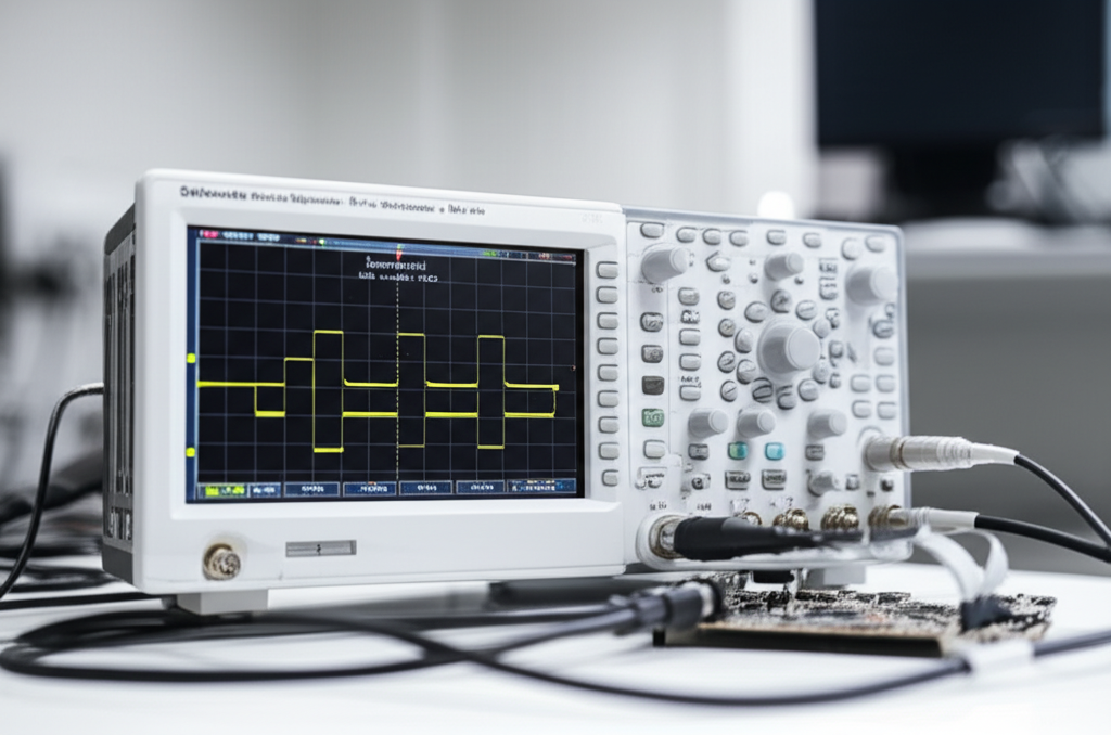
Diploma in Interface JESD204B/C: Architecture and Testing
- Format: Hybrid
- Duration: 6–8 months
- Hours: 800 H
- Language: English / Spanish
- Registration date: 23-10-2026
- Strat date: 03-12-2026
- Available places: 2
1,695 $
Competencies and results
What you will learn
1. Mastering the JESD204B/C Interface: Architecture and Testing
- Understand the architecture and protocol of the JESD204B/C interface.
- Identify and analyze the different functional blocks within a JESD204B/C system.
- Use simulation and analysis tools to validate the JESD204B/C implementation.
- Perform compliance and debugging tests on systems with a JESD204B/C interface.
- Apply advanced techniques for error management and performance improvement in JESD204B/C data transmission.
- Optimize circuit design and signal integrity to maximize the performance of the JESD204B/C interface.
2. In-depth Analysis of JESD204B/C: Design and Verification
## What Will You Learn in the JESD204B/C In-Depth Analysis Course: Design and Verification?
1. Master the fundamentals and evolution of the JESD204 standard, including revisions B and C.
2. Understand the architecture of the JESD204 protocol, including its physical, data link, and transport layers.
3. Analyze in depth the key features of JESD204B/C, such as synchronization, error management, and forward error correction (FEC).
4. Implement simulation models for JESD204B/C link verification, including high-speed channel simulation and performance evaluation.
5. Design and implement design solutions to meet the performance and compliance requirements of the JESD204B/C standard.
6. Use analysis and verification tools, such as protocol analyzers and high-speed test equipment, for design validation.
7. Identify and troubleshoot common problems in JESD204B/C implementation, including signal integrity and timing issues.
8. Understand design considerations for specific applications, such as high-speed data converters, radar systems, and communications.
3. Comprehensive user-oriented design and validation (from modeling to manufacturing)
You will learn to integrate the entire product development process, from initial model conception to final validation, applying user-centered methodologies. You will develop skills in parametric design, ergonomics, simulation, sustainable materials, 3D visualization, and manufacturing management, ensuring efficient, safe solutions that meet current industry standards.
1. Expert Implementation of JESD204B/C: Architecture and Validation
- Master the JESD204B/C interface architecture, understanding its physical, logical, and transport layers.
- Implement data encoding and decoding in JESD204B/C, including scramblers, line encoders/decoders, and CRC.
- Validate the integrity of the JESD204B/C signal through simulation and signal integrity (SI) analysis.
- Configure and program JESD204B/C controllers on FPGAs and ASICs, including handling lane alignment and multi-link configurations.
- Design and optimize PCB layouts to minimize crosstalk and reflections in JESD204B/C signals.
- Use simulation and analysis tools for the verification and validation of JESD204B/C designs.
- Troubleshoot common issues in JESD204B/C implementations, including jitter, data errors, and synchronization problems.
Understand the performance requirements for specific applications, such as high-speed communications, radar systems, and data acquisition.
Apply advanced techniques for jitter mitigation and signal performance improvement in JESD204B/C systems.
5. Master's Degree in JESD204B/C: Architecture and Comprehensive Validation
5. Master’s Degree in JESD204B/C: Architecture and Comprehensive Validation
- Understand the architecture of JESD204B/C systems, including their physical, data link, and application layers.
- Analyze and apply encoding and decoding concepts in JESD204B/C.
- Design and simulate the implementation of JESD204B/C links for different bandwidths and data rates.
- Use simulation and analysis tools to validate the performance and integrity of signals in JESD204B/C links.
- Develop testing and measurement strategies to verify compliance with JESD204B/C specifications.
- Identify and troubleshoot common problems in the implementation of JESD204B/C links, such as synchronization and signal integrity.
- Apply the acquired knowledge to the design of high-speed communication systems, such as data converters, receivers, and transmitters.
- Integrate knowledge of JESD204B/C with other digital communication protocols.
- Stay up-to-date with the latest trends and technologies in the evolution of JESD204.
6. Advanced Implementation of JESD204B/C: Architecture and Effective Testing
6. Advanced Implementation of JESD204B/C: Architecture and Effective Testing
- Understand the complete architecture of JESD204B/C, including the physical, data link, and transport layers.
- Analyze the different operating modes (Lane Rate, Subclass, Scrambling) and their implications for design.
- Master the configuration and programming techniques for JESD204B/C devices, both transmitters and receivers.
- Implement data synchronization and alignment using the various available mechanisms.
- Design high-performance clock systems to optimize performance and signal integrity.
- Use simulation and analysis tools to validate the design and predict performance.
- Develop comprehensive testing strategies, including compliance and stress testing.
- Interpret and analyze test results to identify and solve problems.
- Apply error mitigation techniques and improve system robustness.
- Explore the applications of JESD204B/C in high-speed systems, such as data converters and radio frequency equipment.
Who this program is for:
Diploma in Interface JESD204B/C: Architecture and Testing
- Graduates in Electronic Engineering, Telecommunications, Computer Science, or related fields.
- Professionals in digital systems design, hardware development, and integrated circuit verification.
- RF/microwave engineers, instrumentation, and communication systems who wish to delve deeper into JESD204B/C.
- Experts in testing and measurement, design validation, and signal analysis in high-speed environments.
Recommended requirements: basic knowledge of digital electronics, programming (e.g., Python, VHDL/Verilog); English level B2 or higher.
- Standards-driven curriculum: you will work with CS-27/CS-29, DO-160, DO-178C/DO-254, ARP4754A/ARP4761, ADS-33E-PRF from the first module.
- Accreditable laboratories (EN ISO/IEC 17025) with rotor bench, EMC/Lightning pre-compliance, HIL/SIL, vibrations/acoustics.
- Evidence-oriented TFM: safety case, test plan, compliance dossierand operational limits.
- Mentored by industry: teachers with experience in rotorcraft, tiltrotor, eVTOL/UAM and flight test.
- Flexible modality (hybrid/online), international cohorts and support from SEIUM Career Services.
- Ethics and security: safety-by-design approach, cyber-OT, DIH and compliance as pillars.
1.1 Introduction to the JESD204B/C Interface: Fundamentals and Evolution
1.2 General Architecture of the JESD204B/C: Layers and Components
1.3 JESD204B/C Frame: Data Organization and Encoding
1.4 JESD204B/C Link Configuration: Key Parameters
1.5 Simulation and Modeling of the JESD204B/C Interface
1.6 Analysis and Debugging Tools for JESD204B/C
1.7 Practical Implementation on FPGAs and ASICs
1.8 Design of JESD204B/C Transmitters and Receivers
1.9 Component Selection and System Design
1.10 Case Studies: Applications of the JESD204B/C Interface
1.10
2.2 JESD204B/C Fundamentals: Review of Specifications and Key Concepts
2.2 JESD204B/C System Architecture: Design of Functional Blocks
2.3 JESD204B/C Link Design: Speed and Performance Considerations
2.4 Design and Simulation Tools: Use for Verification
2.5 Design Verification: Simulation and Analysis Techniques
2.6 Jitter and Noise Analysis: Impact on Link Performance
2.7 Signal Integrity: PCB Design and Routing Considerations
2.8 Compliance Testing: Verifying the Design Against Specifications
2.9 Fault Analysis and Troubleshooting: Identifying and Correcting Errors
2.20 Documentation and Design: Generating Design Reports and Documentation
3.3 Introduction to JESD204B/C: Principles and Fundamentals
3.2 JESD204B/C Architecture: Components and Protocols
3.3 JESD204B/C Test Design: Data Generation and Analysis
3.4 JESD204B/C Setup and Testing: Instrumentation and Tools
3.5 JESD204B/C Signal Integrity Analysis: Impact and Mitigation
3.6 JESD204B/C Performance Optimization: Design and Tuning
3.7 JESD204B/C Troubleshooting: Advanced Techniques
3.8 JESD204B/C Practical Applications: Case Studies
3.9 JESD204B/C Simulation: Modeling and Verification
3.30 JESD204B/C Compliance Testing: Certification and Standards
4.4 Validation Fundamentals in JESD204B/C
4.2 Architecture Design for Validation
4.3 Implementing Validation in Design
4.4 Testing and Validation Methodologies
4.5 Validation Tools and Environments
4.6 Results Analysis and Validation Reports
4.7 Data Integrity Validation
4.8 Performance and Compliance Validation
4.9 Interoperability Validation
4.40 Practical Examples and Case Studies in Validation
5.5 Architecture JESD504B/C: In-depth Review
5.5 Physical Layer Design JESD504B/C: Simulation and Optimization
5.3 Advanced Verification JESD504B/C: Emulation and Stress Testing
5.4 Performance Validation JESD504B/C: Signal Analysis
5.5 Complex Integration JESD504B/C: System Design
5.6 Quality Control JESD504B/C: Error Mitigation
5.7 Interoperability Testing JESD504B/C: Connecting with Other Devices
5.8 Simulation Tools JESD504B/C: Modeling and Analysis
5.9 Certification and Compliance JESD504B/C: Industry Standards
5.50 Case Study: Successful Implementation JESD504B/C
6.6 JESD204B/C Fundamentals: Introduction and Protocol
6.2 JESD204B/C Architecture: Transmitter and Receiver Design
6.3 Signal Analysis and Integrity in JESD204B/C Links
6.4 Testing and Validation of JESD204B/C Links: Methods and Tools
6.5 Designing Systems with JESD204B/C: Practical Considerations
6.6 Implementing JESD204B/C on FPGAs and ASICs
6.7 Debugging and Troubleshooting JESD204B/C Systems
6.8 Implementing JESD204B/C: Testing with Professional Equipment
6.9 Performance and Optimization of the JESD204B/C System
6.60 Case Studies: Advanced JESD204B/C Applications
6.7
7.7 Designing and Understanding the JESD204B/C Standard: Architecture and Detailed Specifications
7.2 Implementing the JESD204B/C Physical Layer: Signal Analysis and Performance Optimization
7.3 Implementing and Verifying the JESD204B/C Data Link Layer: Encoding/Decoding and Error Control
7.4 Integrating the JESD204B/C Transport Layer: Data Management and Synchronization
7.7 Thorough Testing and Validation of JESD204B/C Systems: Compliance Testing and Troubleshooting
7.6 Designing High-Performance Systems with JESD204B/C: Optimization for Bandwidth and Low Latency
7.7 Simulation and Analysis Tools for JESD204B/C: Modeling and Verifying Behavior
7.8 Designing and Verifying Complex JESD204B/C Systems: System-Level Integration and Testing
7.9 Advanced Debugging and Troubleshooting Strategies JESD204B/C
7.70 Case Studies and Real-World Applications of JESD204B/C
8.8 Introduction to JESD804B/C: Standards and Applications
8.8 JESD804B/C Architecture: Physical, Data Link, and Transport Layers
8.3 Signals and Protocols: Clocking, Framing, and Control
8.4 Basic Testing: Connection Verification and Signal Quality
8.5 Generating and Analyzing Test Patterns
8.6 Testing Tools: Oscilloscopes, Protocol Analyzers
8.7 Identifying and Troubleshooting Common Problems
8.8 JESD804B/C Link Design: Design Considerations
8.8 Designing JESD804B/C Transmitters and Receivers
8.3 Signal Integrity Analysis
8.4 Link Simulation and Modeling
8.5 RTL Verification: Design and Verification
8.6 Verification Methodologies
8.7 Documentation and Design
8.8 Advanced JESD804B/C Architecture: Link Configuration Complex Systems
3.8 Multi-Device Implementation: Synchronization and Scalability
3.3 Advanced Testing Techniques: Jitter, Eye Diagrams, BER
3.4 Instrumentation and Measurement: Tools and Techniques
3.5 Fault Analysis: Error Identification and Mitigation
3.6 Case Studies: Real-World Implementations
3.7 Performance Optimizations
4.8 FPGA and ASIC Implementation: Design Flows
4.8 Interface Design for ADC/DAC Devices
4.3 Functional Validation: Testbench and Simulation
4.4 Integration Testing: Hardware and Software
4.5 Compliance Verification: Standards and Requirements
4.6 Report Generation and Documentation
4.7 Troubleshooting in the Implementation Process
5.8 Complex Systems Architecture: Subsystem Design
5.8 Implementation of Multiple-Link Systems JESD804B/C
5.3 Analysis of Performance: Delay, Bandwidth, and Power Consumption
5.4 Advanced Testbench Design
5.5 Validation Strategies: Code Coverage and Testing
5.6 Quality Assurance: Validation Process
5.7 Design Optimization for Performance and Reliability
6.8 Effective Testing Strategies: Methodologies
6.8 Design of Automated Test Environments
6.3 Test Data Analysis: Interpretation and Presentation
6.4 Testing Tools: Software and Hardware
6.5 Boundary Testing: Performance Optimization
6.6 Fault Detection and Diagnosis
6.7 Continuous Improvement of the Testing Process
7.8 High-Performance System Architecture
7.8 Design for Different Applications: Communications, Radar
7.3 Performance Validation: Metrics and Measurement
7.4 Signal Integrity Validation: Analysis and Simulation
7.5 Strategies for Testing: Strategies and Coverage
7.6 Documentation and Reporting: Documentation and Presentation
7.7 Quality and Reliability Improvement
8.8 Interface Design: Design Considerations
8.8 Circuit Design: Components and Implementation
8.3 Signal Testing: Testing and Measurement
8.4 Signal Integrity Testing: Design and Verification
8.5 Data Analysis: Interpretation and Troubleshooting
8.6 Testbench Design: Test Automation
8.7 Design for Manufacturing: Optimization
8.8 Design Documentation
8.8 Design Methodologies
8.80 Design Implementation
9.9 Fundamentals of the JESD904B/C Interface: Evolution and Characteristics
9.9 JESD904B/C Architecture: Layers, Functional Blocks, and Key Parameters
9.3 Simulation and Modeling of the JESD904B/C Interface
9.4 Signal Integrity Testing and Noise Analysis
9.5 Tools and Methodologies for Testing in JESD904B/C
9.6 Generation and Analysis of Test Patterns
9.7 Printed Circuit Board (PCB) Design for JESD904B/C
9.8 Instrumentation and Test Equipment for JESD904B/C
9.9 Troubleshooting and Failure Analysis in the JESD904B/C Interface
9.90 Test Results Reporting and Documentation
9.9 Review of the JESD904B/C Standard: Definition and Specifications
9.9 Designing Systems with JESD904B/C: Topologies and Considerations
9.3 Design and Simulation Tools for JESD904B/C
9.4 Functional Verification and Design Simulation
9.5 Physical Layer (PHY) Design for JESD904B/C
9.6 Analysis of Compliance with Specifications and Key Parameters
9.7 Verification Methodologies: Simulation, Hardware Testing
9.8 Performance Verification and Analysis
9.9 Design Review and Validation
9.90 Design Documentation and Verification Process
3.9 JESD904B/C-Based System Architecture: Integration and Challenges
3.9 Designing the JESD904B/C Interface on FPGAs and ASICs
3.3 Physical Layer (PHY) Implementation on FPGA Devices
3.4 Generation and Analysis of Test Patterns for JESD904B/C
3.5 Design of Functional and Performance Tests
3.6 Signal Integrity Testing and Jitter Analysis
3.7 Advanced Instrumentation and Test Equipment
3.8 Performance Optimization and 3.9 Troubleshooting
3.9 Test Results Report and Complete Documentation
3.90 Case Study Analysis and Best Practices
4.9 Planning the Implementation and Validation of the JESD904B/C Interface
4.9 Design and Implementation of the Link Layer
4.3 Implementation of the Data Transport Layer
4.4 Functional Verification and Design Validation
4.5 Design of Interoperability and Compatibility Tests
4.6 Implementation of Stress Tests and Performance Analysis
4.7 Analysis of Results and Design Optimization
4.8 Hardware Validation: Commissioning and Testing
4.9 Troubleshooting and Failure Analysis in Implementation
4.90 Validation Documentation and Report
5.9 Architecture of Complex Systems with JESD904B/C
5.9 Advanced Design of the PHY Layer and Performance Considerations
5.3 Design and Optimization of the Link Layer
5.4 Implementation of Functional Error Correction (FEC) Solutions
5.5 Comprehensive Design Validation: Simulation and Testing Hardware
5.6 Stress Test Design and Performance Analysis
5.7 Advanced Jitter and Noise Analysis Techniques
5.8 Interoperability and Compatibility Validation
5.9 Detailed Reporting and Validation Documentation
5.90 Design Optimization and Complex Problem Solving
6.9 Methodologies for Effective Testing on JESD904B/C
6.9 Designing Specific Test Patterns and Scenarios
6.3 Advanced Instrumentation and Test Equipment
6.4 Results Analysis and Performance Metrics
6.5 Performance Optimization Through Data Analysis
6.6 Test Automation and Test Scripts
6.7 Error Analysis and Troubleshooting
6.8 Advanced Measurement Techniques and Signal Integrity Analysis
6.9 Detailed Test Reporting and Documentation
6.90 Best Practices for Effective and Rapid Testing
7.9 Designing Complex Systems with JESD904B/C: Advanced Architectures
7.9 Physical Layer (PHY) Design and Considerations Performance
7.3 Data Link Design and Error Control
7.4 Comprehensive Design Verification through Simulation and Hardware Testing
7.5 Interoperability and Compatibility Test Design
7.6 Implementation of Stress Tests and Performance Analysis
7.7 Advanced Jitter and Noise Analysis Techniques
7.8 Design Review and Validation
7.9 Complete Design Documentation and Validation Process
7.90 Case Studies and Best Practices
8.9 Design of Systems Based on JESD904B/C
8.9 Implementation of the Physical Layer (PHY) on Specific Devices
8.3 Design of Conformance and Validation Tests
8.4 Advanced Testing Techniques
8.5 Results Analysis and Performance Optimization
8.6 Design and Test Documentation and Reporting
8.7 Implementation of Solutions for Failure Analysis
8.8 Certification Considerations
8.9 Case Studies and Real-Life Examples
8.90 Best Practices and Tips for Design and Testing JESD904B/C
1.1 Mastering the JESD204B/C Interface: Architecture and Testing
1.2 Fundamentals of the JESD204B/C Specification
1.3 JESD204B/C Link Architecture: Components and Functionalities
1.4 Signal Integrity Testing and Error Analysis
1.5 Testing Tools and Methodologies in JESD204B/C
1.6 Test Design for High-Speed Systems
1.7 Interpretation and Analysis of Test Results
2.1 In-Depth Analysis of JESD204B/C: Design and Verification
2.2 Designing JESD204B/C Systems: Key Considerations
2.3 Functional Verification and Simulation in JESD204B/C Environments
2.4 Designing Printed Circuit Boards (PCBs) Optimized for JESD204B/C
2.5 Timing and Synchronization Analysis in JESD204B/C
2.6 Design Simulation and Verification Tools
2.7 Strategies for Error Mitigation and Performance Optimization
3.1 Comprehensive Experience with JESD204B/C: Architecture and Testing
3.2 Architecture of Advanced Systems Based on JESD204B/C
3.3 Implementation of High-Speed Data Acquisition Systems
3.4 Interoperability and Compatibility Testing
3.5 Performance Analysis in Real-World Scenarios
3.6 Troubleshooting and Optimization of JESD204B/C Systems
3.7 Documentation and Reporting of Test Results
4.1 Expert Implementation of JESD204B/C: Architecture and Validation
4.2 Architecture for Implementing JESD204B/C on FPGAs and ASICs
4.3 Design of Clock and Timing Systems for JESD204B/C
4.4 Functional Validation and Conformance Testing
4.5 Integration with Digital Signal Processing (DSP) Systems
4.6 Design for Manufacturing and Testing (DFM/DFT)
4.7 Strategies Debugging and Troubleshooting
5.1 Mastery of JESD204B/C: Architecture and Comprehensive Validation
5.2 Design of Complex Systems Based on JESD204B/C
5.3 Validation of Systems in High-Strength Environments
5.4 Design of Performance and Stress Tests
5.5 Advanced Signal Integrity Analysis
5.6 Power and Performance Optimization
5.7 Creation of Technical Reports and Design Documentation
6.1 Advanced Implementation of JESD204B/C: Architecture and Effective Testing
6.2 Architecture for High-Speed and Broadband Applications
6.3 Design of Automated Tests for JESD204B/C
6.4 Advanced Testing Techniques and Fault Diagnosis
6.5 Analysis of Jitter and Bit Errors
6.6 Implementation of Security in JESD204B/C Systems
6.7 Performance Optimization in High-Density Environments
7.1 Mastery of JESD204B/C: Architecture and Validation
7.2 System Design for Specific Applications (Telecommunications, Radar, etc.)
7.3 Design Validation in Different Operating Scenarios
7.4 Stress Test Design and System Robustness Assessment
7.5 Electromagnetic Compatibility (EMC) Analysis and Mitigation Design
7.6 System Optimization for Low Power Consumption
7.7 Creation of Complete Design and Validation Documentation
8.1 Expert Implementation in JESD204B/C: Design and Testing
8.2 Design of Systems with Multiple JESD204B/C Links
8.3 Design of Performance and Reliability Tests
8.4 Results Analysis and Design Optimization
8.5 Formal Verification Methodologies
8.6 Integration with Control and Management Software Systems
8.7 Preparation of Technical Reports and Complete Project Documentation
- Hands-on methodology: test-before-you-trust, design reviews, failure analysis, compliance evidence.
- Software (depending on licenses/partners): MATLAB/Simulink, Python (NumPy/SciPy), OpenVSP, SU2/OpenFOAM, Nastran/Abaqus, AMESim/Modelica, acoustics tools, planning toolchains DO-178C.
- SEIUM Laboratories: scale rotor bench, vibrations/acoustics, EMC/Lightning pre-compliance, HIL/SIL for AFCS, data acquisition with strain gauging.
- Standards and compliance: EN 9100, 17025, ISO 27001, GDPR.
Capstone-type projects
- JESD204B/C Interface: Design, implementation, and comprehensive testing on FPGA/ASIC.
- JESD204B/C Analysis: Modeling, simulation, and verification of the complete architecture.
- JESD204B/C Validation: Implementation and testing with performance analysis in complex environments.
- JESD204B/C Architecture: Advanced design and testing strategies to guarantee performance.
- JESD204B/C Implementation: Architecture, comprehensive validation, and optimization of the interface.
- JESD204B/C Interface: Design, simulation, and validation of a high-speed link.
- JESD204B/C Analysis: Implementation of a receiver/transmitter.
- JESD204B/C Experience: Design and implementation of a complete system.
- JESD204B/C Implementation: Functional validation, performance testing, and optimization.
- JESD204B/C Mastery: Development of a complete and robust solution.
- JESD204B/C Advanced: Integration into complex systems, failure analysis.
- JESD204B/C Mastery: Performance optimization and reduction of errors.
- JESD204B/C Expert: Design and validation of high-performance systems.
- JESD204B/C Architecture: Design and implementation of a high-speed serial interface.
- JESD204B/C Verification: Simulations and validation tests on an FPGA.
- JESD204B/C Implementation: Communication testing and performance analysis.
- JESD204B/C Validation: Design and execution of stress tests and data analysis.
JESD204B/C Validation: Design and execution of stress tests and data analysis.
- JESD204B/C Design: Architecture simulation and validation.
- JESD204B/C Testing: Implementation of comprehensive tests.
- JESD204B/C Analysis: Use case development and verification.
- JESD204B/C Implementation: RTL design and testbench.
Admissions, fees and scholarships
- Profile: Background in Computer Engineering, Mathematics, Statistics, or related fields; practical experience in NLP and valued information retrieval systems.
- Documentation: Updated CV, academic transcript, SOP/statement of purpose, project examples or code (optional).
- Process: Application → Technical evaluation of profile and experience → Technical interview → Review of case studies → Final decision → Enrollment.
- Fees:
- Single payment: 10% discount.
- Payment in 3 installments: No fees; 30% upon registration + 2 equal monthly payments of the remaining 35%.
Monthly payment: available with a 7% commission on the total; annual review.
Scholarships: based on academic merit, financial need, and promoting inclusion; agreements with companies in the sector for partial or full scholarships.
See “Calendar & Calls for Applications,” “Scholarships & Grants,” and “Fees & Financing” in the SEIUM mega-menu.
Do you have any questions?
Our team is ready to help you. Contact us and we’ll get back to you as soon as possible.