

Diploma in Stackups, Impedance and Routing Rules
About us Diploma in Stackups, Impedance and Routing Rules
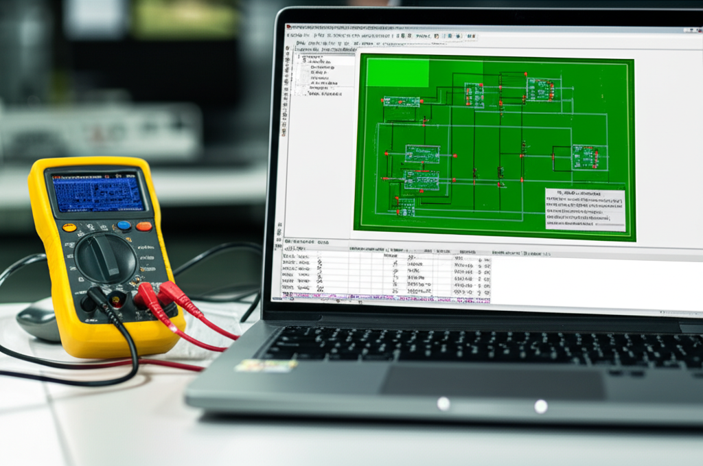
The Diploma in Stackups, Impedance, and Routing Rules provides specialized training in the design and analysis of printed circuit boards (PCBs), focusing on high-speed signal management. It centers on understanding characteristic impedance, designing multilayer stackups, and rigorously applying routing rules to ensure signal integrity and optimal circuit performance. Topics such as signal simulation, crosstalk mitigation, and via optimization are covered, using specialized PCB design software.
The program includes the study of PCB materials, the impact of tolerances, and manufacturing processes, enabling participants to develop practical skills for creating robust and efficient designs.
It focuses on the application of simulation tools and the interpretation of results for design validation. This training prepares electronic engineers and PCB designers to meet the challenges of modern circuit design, from the prototyping stage to mass production, while adhering to industry standards.
Target keywords (naturally occurring in the text): PCB design, stackups, impedance, routing rules, signal integrity, circuit analysis, PCB simulation, PCB materials, design software, electronics diploma.
Diploma in Stackups, Impedance and Routing Rules
- Format:
- Duration:
- Hours: 900 H
- Language:
- Credits:
- Registration date: 08-09-2026
- Strat date: 19-10-2026
- Available places: 8
1,799 $
Competencies and results
What you will learn
Who this program is for:
Diploma in Stackups, Impedance and Routing Rules
9.9 Introduction to Stackups: Layers, Materials, and Configurations
9.9 Characteristic Impedance Calculation and Simulation
9.3 Signal Routing Principles: Basic Rules and Best Practices
9.4 Design for Signal Integrity: Minimizing Reflections and Crosstalk
9.5 PCB Design Tools: Software and Workflows
9.9 Impedance Control Strategies: Tolerances and Variations
9.9 Stackup Optimization for Different Applications: RF, Digital, Analog
9.3 Power and Ground Plane Design: Noise and Filtering
9.4 Signal Integrity Analysis: Eye Diagrams and Simulations
9.5 Advanced Routing Techniques: Vias, Escapes, and Microvias
3.9 Multilayer Stackup Design: Manufacturing Considerations
3.9 High-Frequency Material Selection: Laminates and Prepregs
3.3 Flexible and Rigid-Flex PCB Design: Special Applications
3.4 Power Integrity in High-Speed Designs: Decoupling and Bypass
3.5 Rapid Prototyping and Design Validation
4.9 Fundamental PCB Concepts: Components, Traces, and Pads
4.9 Impedance Analysis and Its Impact on Circuit Performance
4.3 Designing Stackups to Reduce Noise and Interference
4.4 Component Selection and Its Impact on PCB Design
4.5 Practical Applications: Designing PCBs for Different Industries
5.9 Principles of Electronic Circuit Design: Passive and Active Components
5.9 Designing and Analyzing Power Supply Circuits: Regulation and Filtering
5.3 Designing Analog Circuits: Amplifiers, Filters, and Oscillators
5.4 Designing Digital Circuits: Logic Gates, Flip-Flops, and Counters
5.5 System Integration: Connectors, Interfaces, and Communication
6.9 Designing High-Density PCBs: Microvias, Shielding, and Advanced Routing
6.9 Design for Manufacturing (DFM) and Assembly (DFA)
6.3 Designing PCBs for EMI/EMC Environments: Mitigation and Protection
6.4 Design of PCBs for Radio Frequency (RF) Applications: Antennas and Transmission Lines
6.5 Implementing Design Testing and Verification
7.9 Designing PCBs for High-Temperature and Vibration Environments
7.9 Designing PCBs for Military and Aerospace Applications
7.3 Designing PCBs for Medical Applications: Safety and Reliability
7.4 Thermal Analysis and Heat Dissipation Management
7.5 Designing Waterproof and Corrosion-Resistant PCBs
8.9 Designing High-Speed PCBs: Data Rates and Rise Times
8.9 Signal Integrity Analysis in High-Speed Designs
8.3 Routing Techniques to Minimize Crosstalk
8.4 Designing Power and Ground Planes to Reduce Noise
8.5 Simulating and Optimizing High-Speed Designs
9.9 Advanced Material Selection for Stackups
9.9 Design Considerations for Different Signal Types
9.3 Impact of Stackup Design on Manufacturing and Cost
9.4 Stackup Simulation and Analysis Techniques
9.5 Stackup design for different applications (e.g., IoT, automotive)
9.6 Integrating the stackup design with the overall PCB design
9.7 Future trends in stackup design
9.8 Tools and software for stackup design
9.9 Case studies and practical examples
9.90 Stackup design optimization and validation
9.1
Capstone-type projects
- High-Speed PCB: Optimized design for fast signals, SI/PI analysis.
- Advanced Stackup: Multilayer stackup design with precise impedance control.
- Strategic Routing: Advanced techniques to minimize interference and noise.
- Simulation and Validation: EMI/EMC analysis and design optimization.
Admissions, fees and scholarships
Do you have any questions?
Our team is ready to help you. Contact us and we’ll get back to you as soon as possible.